


×
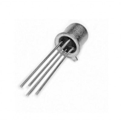
BFW10 Semiconductor Device
A semiconductor device for amplifying or switching electronic signals and power.
- Transistor Polarity: N-Channel
- Drain-Source Voltage (VDS): 30VDC
- Drain-Gate Voltage (VDG): 30VDC
- Reverse Gate-Source Voltage (VGSR): 30VDC
- Forward Gate Current (IGF): 10mA
- Gate-Source Cut-off Voltage (VGS(off)): 8VDC
- Gate-Source Voltage (VGS): 7.5VDC
- Zero-Gate Voltage Drain Current (IDSS): 20mA
- Operating Temperature Range: -65 - 150°C
- Power Dissipation (PD): 300mW
Features:
- Metal TO-72 can package
- Advanced process technology
- Low error voltage
- Fast switching speed
It is composed of semiconductor material with at least three terminals for external circuit connection. The transistor's terminals control the current through another pair based on the applied voltage or current. With higher output power than input power, it can amplify signals. Transistors can be individually packaged or embedded in integrated circuits.
Related Documents: BFW10 JFET Datasheet
* Images are for illustration only; actual product may vary.