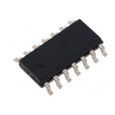
CD4093 Schmitt-Trigger Circuit
Four Schmitt-trigger circuits with wide supply voltage range and noise immunity
- DC Supply Voltage: 3.0V to 15V
- Input Voltage: -0.5 to VDD + 0.5V
- Storage Temperature: -65°C to +150°C
- Power Dissipation: 700 mW
- Lead Temperature: 260°C
- Pack/Unit: 1 piece
Top Features:
- Wide supply voltage range: 3.0V to 15V
- Schmitt-trigger on each input with no external components
- Noise immunity greater than 50%
- Equal source and sink currents
The CD4093 consists of four Schmitt-trigger circuits, each functioning as a 2-input NAND gate with Schmitt-trigger action on both inputs. The gate switches at different points for positive and negative-going signals, with hysteresis voltage (VH) defined as the difference between the positive (VT +) and negative voltage (VT -).
All outputs have equal source and sink currents and conform to standard B-series output drive. There is no limit on input rise and fall time, and the hysteresis voltage for any input is specified at TA = 25°C.
Applications:
- Wave and pulse shapers
- High-noise-environment systems
- Monostable multivibrators
- Astable multivibrators
- NAND logic
Ordering Code Specification: Symbol Parameter Values VDD DC Supply Voltage -0.5V to +20V VIN Input Voltage -0.5 to VDD + 0.5 VDC TS Storage Temperature -65°C to +150°C PD Power Dissipation 700 mW TL Lead Temperature 260°C
Related Document: CD4093 SMD Data Sheet
* Images are for illustration only; actual product may vary.

